


The photodiode is a special diode that converts the light signal into a current or voltage signal. Its structure is basically the same as that of a traditional diode. It has a PN junction. However, when designing and manufacturing the photodiode, try to make the area of the PN junction smaller. Large, in order to receive incident light. Its basic principle is: when light hits the photodiode, the absorbed light energy is converted into electrical energy. The photodiode works under reverse

In self-driving cars, lidar plays a key detection and guidance role. In fact, the more advanced and sensitive the device is, the more accurate the detected signals will be, and the more significant the application advantage in actual driving. In the research of this equipment, adding a near-infrared silicon photodiode can improve its sensitivity. Next, I will discuss with you the role of near-infrared silicon photodiode in lidar. Near-infrared silicon photodiode, its sensitivity is one-third h

PIN photodiode is a kind of semiconductor device made of P-I-N structure, which can convert optical signal into electrical signal, and can change with the change of light. In view of the shortcomings of conventional PD, its structure has been improved, and its sensitivity is higher than that of conventional P-N junction photodiodes, and it has unidirectional conductivity characteristics. The commonly used silicon photovoltaic cells in the market generally work in the visible light band. The p

Household appliances are an indispensable part of our daily lives. Most household appliances are inseparable from photodiode semiconductor devices. They are also widely used in medical, industrial, and scientific research equipment. Next, the editor will give a brief introduction to photodiodes. The photodiode is basically the same as other photosensitive elements, and has quite a lot of applications with the photodiode in the function of the photosensitive element and the photosensitive resist
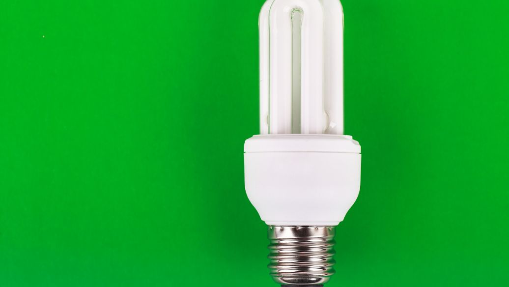
Since the discovery of graphene materials, optoelectronic devices based on two-dimensional materials have been extensively studied due to their unique electrical and optical properties, and have shown great potential in the fields of photodetectors and solar cells. In this, all kinds of photodiodes are indispensable. Next, I will discuss with you what the photodiode of the high-performance photodetector is like.A good photodetector should have the advantages of fast response, short response tim

What is an uncooled "nanowire" short-wave infrared photodiode? The term is very long, and it seems a bit difficult to understand, but in fact, this is only one of the photodiodes, and it is proposed for the application of infrared sensors that cannot be separated from cooling and other restrictions. Next, I will discuss this kind of component with you. The problem of refrigeration has always been a concern of infrared sensor researchers. The SWIR and MWIR detectors that are not cooled

At present, due to the high cost of epitaxial semiconductors, the application versatility of infrared multi-spectral imaging detectors is somewhat affected. In comparison, colloidal quantum dots (CQD) that can be processed in a solution and can be adjusted in a broad spectrum are more suitable for manufacturing a variety of low-cost and high-performance optoelectronic devices. The double-ended colloidal quantum dot dual-band detector is used to achieve dual-band infrared imaging. In this dete

High-speed optoelectronic semiconductor devices are embedded in the optical fiber, including LED and photodiode detectors, making it a cleanable soft fabric for communication systems. Next, the editor will mainly talk to you about the application research of photodiodes in the cleaning of soft fabrics in communication systems. Traditionally, an optical fiber is composed of a cylindrical object called a "preform"-this object is basically an amplified optical fiber. Then the preform i

Whether it is a large data center or millions of supercomputers, high-bandwidth and high-efficiency optical interconnections are required. Therefore, the silicon optical interconnection technology has attracted much attention due to its high integration and low cost advantages. The high-order modulation code pattern can further increase the data rate under the limited bandwidth of integrated circuits or optical devices, so it is more and more favored by academia and the industry. However,
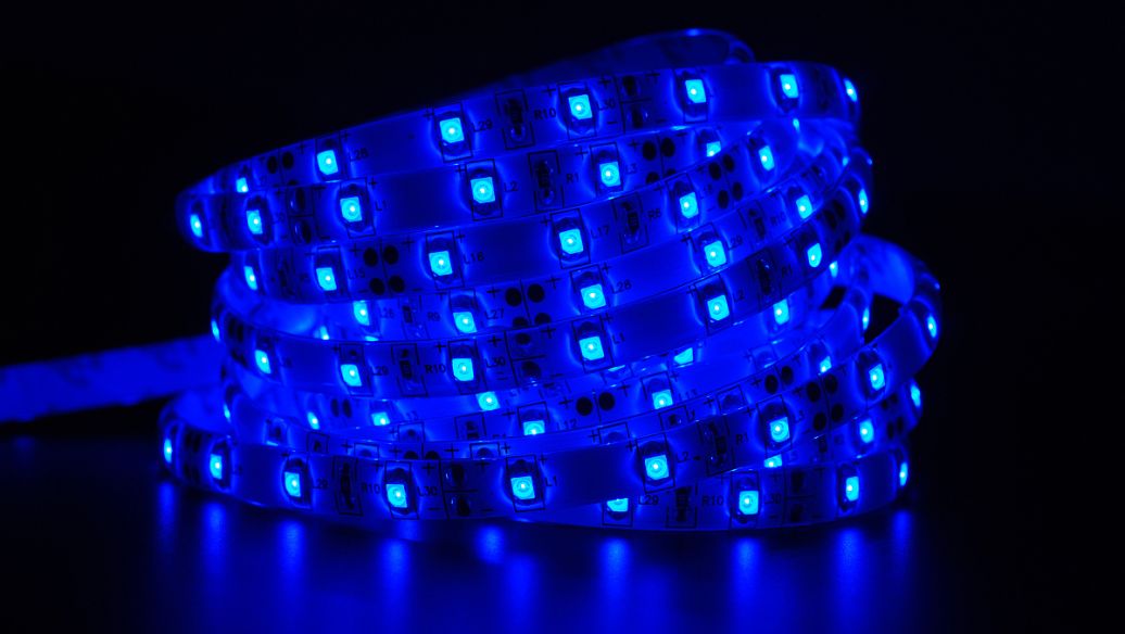
Infrared emission tube is a kind of expressible luminous body material composed of infrared light-emitting diodes used after a series of operations. When this product is produced, it needs to use existing materials with high infrared radiation efficiency, such as gallium arsenide, which is commonly used. Then we use this to make a PN junction, where the forward bias will inject current into the PN junction to excite infrared light. After we do this, the approximate spectral power of the infrared
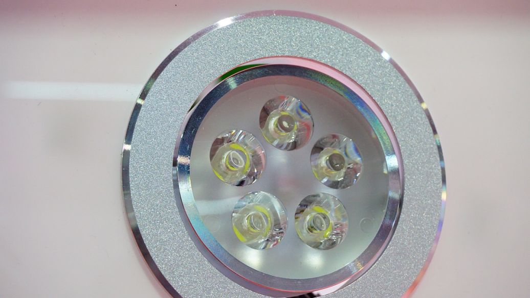
Large area 800μm diameter 4H-polysilicon carbide ultraviolet (UV) avalanche photodiode, with high gain (106), high quantum efficiency (81.5%), low dark current intensity, and high UV/visible light rejection ratio. In this product, the variable temperature photoresist reflow technology is used for the first time to produce smooth beveled sidewalls, which can suppress leakage current and avoid premature edge breakdown. Ultraviolet detection has a wide range of applications in astronomy, c

Infrared emitting tube is also called infrared emitting diode. It is a light-emitting device that can directly convert electrical energy into near-infrared light and radiate out at the same time. It is widely used in Bluetooth, computer wireless data transmission, LED industry, household appliances, medical appliances, cameras, Camera etc. 1. The appearance is exquisite and flawlessThe good quality infrared emitting tube has no flaws in appearance, and the production is relatively delicate. It